Introduction
Photonics and optoelectronics are at the heart of modern technology, powering applications ranging from high-speed internet and smartphones to medical imaging, sensors, and renewable energy systems. As the demand grows for faster, smaller, and more energy-efficient devices, traditional materials such as silicon face physical and performance limitations. In this context, Single-Walled Carbon Nanotubes (SWCNTs) have emerged as a transformative nanomaterial, offering unique optical and electronic properties ideally suited for next-generation photonic and optoelectronic applications.
SWCNTs, which are cylindrical structures formed from a single layer of graphene, exhibit remarkable interactions with light across a wide range of wavelengths. Their tunable bandgaps, strong light–matter interaction, ultrafast response times, and nanoscale dimensions make them a powerful platform for innovation in photonics and optoelectronics.
Understanding Single-Walled Carbon Nanotubes
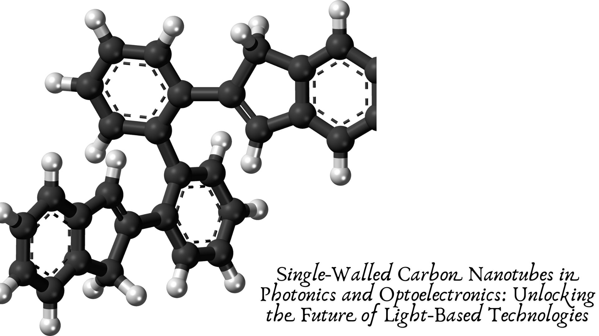
Single-walled carbon nanotubes consist of a single sheet of carbon atoms arranged in a hexagonal lattice and rolled into a seamless tube with diameters typically between 0.7 and 2 nanometers. Their properties depend strongly on their chirality—the way the graphene sheet is rolled—which determines whether a nanotube behaves as a metal or a semiconductor.
This chirality-dependent electronic structure is particularly important in photonics and optoelectronics, where precise control over light absorption, emission, and modulation is essential. Semiconducting SWCNTs, in particular, are highly valuable because their direct bandgaps allow efficient interaction with photons.
Unique Optical Properties of SWCNTs
One of the most compelling reasons SWCNTs are attracting attention in photonics is their exceptional optical behavior.
Strong Light Absorption
SWCNTs exhibit sharp and well-defined optical absorption peaks associated with excitonic transitions. These strong absorption features span the visible, near-infrared (NIR), and infrared regions, making SWCNTs suitable for broadband photonic devices.
Photoluminescence
Semiconducting SWCNTs can emit light when excited, producing photoluminescence in the near-infrared region. This property is particularly valuable for applications such as optical communications, bioimaging, and infrared light sources.
Ultrafast Optical Response
SWCNTs respond to optical excitation on femtosecond to picosecond timescales, enabling ultrafast modulation and signal processing. This makes them ideal for high-speed optoelectronic components.
SWCNTs in Photonic Devices
The integration of SWCNTs into photonic systems has opened new avenues for device design and performance enhancement.
Optical Modulators
SWCNT-based optical modulators leverage changes in absorption or refractive index under an applied electrical or optical signal. Their fast carrier dynamics allow modulation at extremely high speeds, which is crucial for next-generation optical communication networks.
Waveguides and Integrated Photonics
Due to their nanoscale dimensions and compatibility with flexible substrates, SWCNTs can be integrated into photonic waveguides and on-chip photonic circuits. They enable miniaturization while maintaining strong light–matter interaction.
Saturable Absorbers for Lasers
SWCNTs are widely used as saturable absorbers in ultrafast lasers. Their broadband absorption and fast recovery time make them effective for generating short laser pulses, including mode-locked and Q-switched lasers.
Applications in Optoelectronics
Beyond purely photonic components, SWCNTs play a critical role in optoelectronic devices that convert light into electrical signals and vice versa.
Photodetectors
SWCNT-based photodetectors exhibit high sensitivity, fast response times, and broadband detection capabilities. They are particularly effective in the near-infrared range, where traditional silicon detectors struggle.
Light-Emitting Devices (LEDs)
SWCNTs are being explored for use in nanoscale light-emitting devices. Their tunable emission wavelengths enable customized optical outputs, which is valuable for displays, optical signaling, and sensing applications.
Solar Cells
In photovoltaic devices, SWCNTs serve as light absorbers, charge transport layers, or transparent electrodes. Their high electrical conductivity and strong optical absorption contribute to improved charge separation and collection, enhancing overall device efficiency.
Advantages Over Conventional Materials
SWCNTs offer several advantages compared to traditional photonic and optoelectronic materials:
- Broad spectral tunability from visible to infrared
- High carrier mobility for efficient charge transport
- Mechanical flexibility, enabling bendable and wearable optoelectronic devices
- Low power consumption due to efficient light–matter interaction
- Compatibility with solution processing, allowing scalable and cost-effective fabrication
These advantages position SWCNTs as strong candidates for replacing or complementing silicon and other conventional semiconductors in advanced applications.
Challenges in SWCNT-Based Photonics
Despite their promise, several challenges must be addressed before SWCNTs achieve widespread commercial adoption:
- Chirality control: Separating metallic and semiconducting nanotubes remains complex
- Uniformity and reproducibility in large-area device fabrication
- Integration with existing manufacturing processes
- Stability and long-term performance under operating conditions
Ongoing research in material purification, alignment techniques, and hybrid device architectures continues to overcome these limitations.
Future Outlook
The future of single-walled carbon nanotubes in photonics and optoelectronics is highly promising. Advances in controlled synthesis, scalable processing, and device integration are accelerating their transition from laboratory research to real-world applications. Emerging fields such as quantum photonics, neuromorphic computing, and wearable optoelectronics are expected to benefit significantly from SWCNT-based components.
As demand grows for faster communication systems, compact photonic circuits, and energy-efficient optoelectronic devices, SWCNTs are poised to play a pivotal role in shaping the next generation of light-based technologies.
Conclusion
Single-walled carbon nanotubes represent a powerful and versatile material platform for photonics and optoelectronics. Their exceptional optical properties, ultrafast response, and nanoscale dimensions enable innovative device designs that surpass the limitations of traditional materials. While challenges remain, continued research and technological advancements are steadily unlocking the full potential of SWCNTs, paving the way for transformative breakthroughs in how light is generated, controlled, and converted in modern technology.
If you’d like, I can also tailor this article for SEO, adapt it for a research-focused audience, or localize it for industrial and commercial applications.